

Layout finishing of a 28nm, 3 billions transistors and multi-core...
Resources, white papers, articles
Layout finishing of a 28nm, 3 billions transistors and multi-core processor
Philippe Morey, Eric Beisser
XYALIS – Grenoble – France
Conference: Photomask and NGL Mask Technology, June, 2013, Yokohama, Japan
ABSTRACT
Designing a fully new 256 cores processor is a great challenge for a fabless startup. In addition to all architecture, functionalities and timing issues, the layout by itself is a bottleneck due to all the process constraints of a 28nm technology. As developers of advanced layout finishing solutions, we were involved in the design flow of this huge chip with its 3 billions transistors. We had to face the issue of dummy patterns instantiation with respect to design constraints. All the design rules to generate the “dummies” are clearly defined in the Design Rule Manual, and some automatic procedures are provided by the foundry itself, but these routines don’t take care of the designer requests.
Such a chip, embeds both digital parts and analog modules for clock and power management. These two different type of designs have each their own set of constraints. In both cases, the insertion of dummies should not introduce unexpected variations leading to malfunctions. For example, on digital parts were signal race conditions are critical on long wires or bus, introduction of uncontrolled parasitic along these nets are highly critical. For analog devices such as high frequency and high sensitivity comparators, the exact symmetry of the two parts of a current mirror generator should be guaranteed. Thanks to the easily customizable features of our dummies insertion tool, we were able to configure it in order to meet all the designer requirements as well as the process constraints. This paper will present all these advanced key features as well as the layout tricks used to fulfill all requirements.
CONSTRAINTS
When performing the layout of any chip, the main set of constraints come from the foundry according to the process specifications. Every constraint is described in the Design Rule Manual. For a 28nm process, many constraints should be met for dummy geometries insertion. We have first, local constraints based on design rules such as spacing and sizes of drawn patterns. This implies that dummy patterns should carefully meet specifications about their shape (width, height, area, aspect ratio…). We then have intra layer density constraints. These constraints may be quite complex:
- global density constraint at chip level
- local density constraint within a window
- density variation between adjacent windows[1]
In each case, constraints are made of a minimum and a maximum value.
At 28nm node, some inter layer density constraints also start to appear. They will certainly become a key point in future technology nodes (22nm and beyond). With these constraints, not only density constraints should be met for a given process layer, but average densities across multiple layers should be met. As an example, layer 1 and layer 2 should reach a density between 30% and 80%, but the average density of layer 1 and 2 should not exceed 70%. Additionally, it seems that the size of the windows on which these constraints should be met, may vary depending on the layer. Hopefully, we didn’t have to face such complex constraints in our case, but this has led to work on new features for the next generation of the dummies insertion engine.
In addition to all these constraints, we have to take into account some spacing or exclusion rules with specific layers which may be physical or virtual. We were also faced with a combination of geometrical constraints and density constraints. The goal was to instantiate two types of dummy patterns, “small” ones at a given distance of active geometries, and “big” ones at another distance (generally larger). We also had to reach a given density of polysilicon as well as a given density of transistors. This implies to identify and manage separately some specific structures. It is important to notice that all process constraints are mandatory. They are all specified in a design rule manual and checked by a DRC. Our goal was to have a 100% error free layout without any waiver.
Design constraints
In all nowadays System On Chip, we have both digital and analog parts. The design constraints will differ depending on the block type. Obviously, the impact of the dummies on the design should be as low as possible in both cases, but we will have specific constraints. The multi-processor array chip, with its 256 cores embed a huge amount of digital blocks, but also many analog blocks for power management, clock control, input/output interfaces, etc…[3]
Regarding analog blocks, we often found symmetrical devices to build high sensitivity comparators or amplifiers. The schematics of such functions are made of 2 identical branches but the layout by itself is drawn with two strictly symmetrical branches. Any difference between the two branches may lead to dramatic results in terms of performances of the full function. In this case, all additional device, including parasitic ones, should be placed in the same way in both branches. It is then important to first identify the areas on which such placement of dummy geometries is required, and then to have a tool able to handle such constraints.
Regarding digital blocks, usually the core by itself is dense enough in lower levels to meet density constraints, and it is generally impossible to add any extra geometries at these levels inside digital blocks. The problem occurs between digital blocks or at upper interconnection layers where we mostly find busses. The signals running on these busses are subject to race conditions. It is important to have all the bits of the data transferred by such interconnection arriving at the same time[7]. This problem is fixed during the synthesis phase of the design and by the Place & Route tool when detailed timing conditions are specified. But once the dummy patterns have been inserted, many parasitics capacitors are”randomly” added and may lead to critical delays on wires. It is then, important to address this issue during dummies instantiation and keep a parasitic balancing on the interconnection wires.
Another request from the designers was the possibility to interconnect the dummies. This allows to make a better model of the parasitic devices: one large capacitor is much more easier to simulate than thousands of small ones, especially if they are grounded.
Workflow constraints
According to previous constraints, it is important for the designer to have a tool that could be easily customizable. Most of the flows provided by foundries are made to meet all process constraints but can’t be modified by the designer, so that all the above mentioned issues can’t be fixed automatically. In this case, insertion of dummies should be made manually in critical cases. This implies, first that the tool can easily take into account all the process constraints, and then can be easily configured by the designer to take into account his constraint while sill meeting process rules.
Another issue of the design CAD flow, is the size and complexity of the data. Designing a 3 billion transistors System On Chip implies huge data bases. This means that the engine used for dummy patterns instantiation should be able to handle many giga bytes of data within the shortest possible time. Some iterations are expected because it may not be possible to reach the density target on the first run: following the local design rules may not allow to place enough dummy structures. It is not acceptable for the designer to spend days to converge on this layout step.
Finally, the last challenge was about the final database size. Starting with a 40Gb layout database, will often lead to a more than 100Gb database with the dummies. This becomes unacceptable. It is important to optimize the resulting database in order to get the smallest possible size. This may save a lot of time for further operations such as DRC and at least data transfer.
DUMMY PATTERNS INSERTION SOLUTIONS
A dedicated engine
A commercial dedicated tool for dummies insertion was available for years and successfully used on “older” technology nodes: 65nm and 45nm. The challenge was to check how it can meet the requirements of a 28nm process with the complexity of a very big design. The tool basically provides all the features requested in the above mentioned constraints. It has been carefully parameterized to fulfill all the foundry specifications. Specific options have been used to follow the designer expectations. For digital blocks and race condition issues on long wires, a dedicated option allows to instantiate the dummy patterns on non orthogonal grids.
The dummy geometries, by themselves, are placed without any rotation, but two contiguous dummy patterns are placed with a slight horizontal and/or vertical shift. This allows a better repartition of the induced parasitics capacitors. In case of orthogonally placed dummies, you may find a full row of dummies placed closely to one wire, while another wire may be far from next row of dummies. Thanks to non orthogonal placement, the average distance between dummy geometries (i.e. parasitic capacitors) is almost the same for all wires.
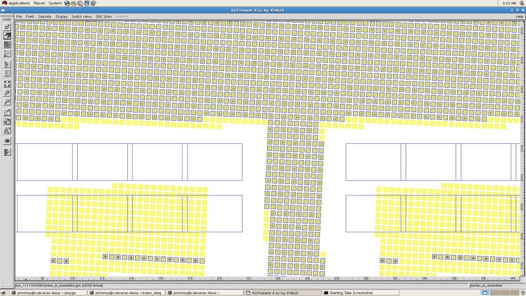
Figure 1. Non orthogonal placement of dummy metal patterns
Another important feature is the ability to interconnect the generated dummy patterns. This can be done in one or all of the 3 directions: either in X and/or Y within the same layer, or vertically between current and lower and/or upper process layer with vias. This additional step is fully automatic and do not need extra computation time.
Dummy cells layout
In addition to the generation of simple rectangular dummy shapes, the tool is able to instantiate complex cells. This feature is very helpful to instantiate dummy transistors as it is possible to instantiate directly a complex cell including N-Mos, P-Mos and simple polysilicon geometries.
The most important challenge was to clearly understand the dummies generation rules and to convert them into a constraint file and a set of pre-drawn dummy cells. Figure 2 shows how two different kind of cells including both N and P transistors as well as simple polysilicon shapes.
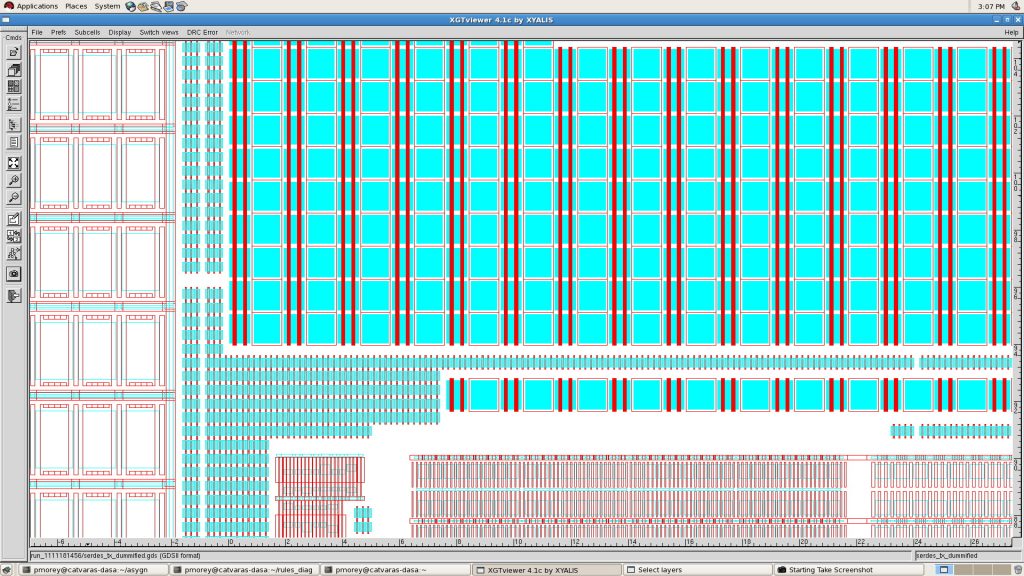
Figure 2. Complex cells with transistors
The size and the exact layout of the dummy cells is a trade off between an homogeneous distribution of dummy shapes and devices, and the ability to insert dummies in any free area in order to reach the density goal. Drawing the smallest possible cell will greatly simplify its insertion in any small empty areas but may not allow to reach the expected density. For example, if the minimum spacing between dummies is 0.5um, a 0.5um X 0.5um dummy cell will only allow to obtain 25% of density in a large empty area, while a 1.5um X 1.5um will allow to obtain 56% of density in the same area. Some iterations in the setup process were needed to find the best trade off. If no universal solution can be found, the process should be run in two steps. In first step we will fill all empty areas with “big” dummy cells but with a large spacing with active geometries so that only large empty areas will be filled. In a second step we fill all remaining empty areas at the minimum spacing distance with “small” dummy cells. Figure 2 shows this kind of implementation. An additional feature of the tool allows to merge small shapes into bigger ones when they are adjacent, but all the density constraints were successfully met without using this option.
Programming complex functionality’s
The dummies instantiation engine directly provides all the common features, but in some cases, it is important for the designer, to be able to program some specific procedures. Instead of providing a tool dependent language with some restrictions, a set of commands to manipulate the layout databases are available from Unix and can be called from any scripting language. In order to fix all design specific issues such as the instantiation of symmetrical dummies in some areas of analog blocks, a set of user friendly commands are available. The miscellaneous functions that have been used are:
- extraction of the coordinates of the areas in which dummies should be instantiated symmetrically
- flip of analog cells
- constrained dummies instantiation
- merge of mirrored and standard dummy patterns
Different datatypes on area recognition layer where used to identify horizontal or vertical mirror. All the calls to the different tools were embedded in a simple shell script. Figure 3 shows a small example of a cell on which dummies should be generated symmetrically around a vertical axis.
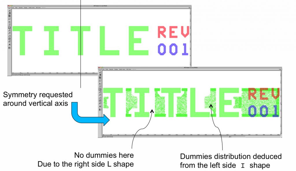
Figure 3. Mirrored dummies
The distribution of the dummies is also a key point[6]. You can notice in figure 3, that the dummies are not distributed homogeneously in the free areas. The expected amount of dummy patterns has been generated to reach the density target but they are placed far enough from active geometries when possible. This is a specific “keep away” feature of the tool that has been used.
DUMMIES GENERATION RESULTS
Quality
With its first time good silicon, the design flow of this Multiple Parallel Processor Array with 256 cores has proved its robustness. The dummies generation flow provided by the foundry was not used for this design because of its lacks of flexibility. The designer didn’t have any control on the result and this was clearly a blocking point to reach the expected performances of the chip. The flow that has been put in place uses another tool with a significantly different algorithm compared to what is commonly used[4, 5]. The results were the ones expected by the designers, both in terms of layout and in terms of efficiency. The quality of the final layout has been first checked with the standard DRC provided by the foundry and finally with the silicon. Next table shows the various constraints we had to face and the results obtained.
| Constraint | Result |
|---|---|
| Follow all design rules provide by the foundry | Yes |
| Quickly configure the tool | ~ 8 days |
| Meet designers requests | Through existing options for top level and digital blocks. With shell scripting for analog blocks |
| Run in a very short time | < 1 night for full processing of a 33Gb database |
| Generate small data bases | Size increase ~ 10% |
Performances
The first version of the dummies generation tool used to process the layout database was not using parallelism. The whole processing time has been shortened by running the different layers in parallel with fully independent process. A new version, fully using the capacities of multi-core workstations has been released. The performances have been greatly improved, decreasing from about 20h for processing the most complicated layer (metal 1) down to about 1h for 1 pass. Management of the different steps to generate the dummies on all the layers has been fully automatized. It is now possible to enter all the rules for all the layers at once, and the tool will distribute the tasks to the available processors in order to obtain the result in the shortest possible time.
Following table shows the performance on the different layers.
| Layer | CPU time |
|---|---|
| Poly + Active: 2 pass with different dummy cells | 53 mn |
| Thin metals: 6 layers X 3 pass with diagonal dummies | 306 mn |
| All metals with gradient fix: 8layers X 2 pass | 363 mn |
| Vias and dummies interlayer connections: 6 layers | < 1mn |
This makes a total of about 12 hours to get a fully DRC clean data base with regards to design constraints such as parasitics reduction and net balancing. The size of GDSII data base grown from 33Gb to 37Gb. This is about 10% of increase for all the dummies in 15 different layers: active, poly, 8 metals and 5 vias.
Acknowledgments
We would like to warmly thanks Kalray’s (KALRAY) design team for their collaboration in the validation of our layout finishing flow. Getting a first time good silicon on such a complex chip is the best recognition we all can have expected.[2]
Conclusion
Being involved in the design of such a big chip in one of the most advanced technologies was a great challenge. The first samples of the chip are fully functional and meet all expected performances.
The tool that has been used has already proven its robustness since many years, but with this test case, it has also proved its efficiency, flexibility and capability to cover all the needs of new processes. The engine has been improved to achieve unsurpassed performances by using parallelism. New features have been added to the roadmap in order to address the problem of multi layers combined constraints.
References
[1] Huang-Yu Chen, Szu-Jui Chou, and Yao-Wen Chang. Density gradient minimization with coupling-constrained dummy fill for cmp control. In Proceedings of the 19th international symposium on Physical design, ISPD ’10, pages 105–111, New York, NY, USA, 2010. ACM.
[2] Space Daily. European investments in advanced computing systems deliver results, february 2013.
[3] Benoit Dupont de Dinechin. Integrating a distributed memory computer on a chip: challenges and opportunities. In HiPEAC, editor, HiPEAC. HiPEAC, February 2013.
[4] Chunyang Feng, Hai Zhou, Changhao Yan, Jun Tao, and Xuan Zeng. Provably good and practically efficient algorithms for cmp dummy fill. In Proceedings of the 46th Annual Design Automation Conference, DAC ’09, pages 539–544, New York, NY, USA, 2009. ACM.
[5] Aditya P. Karmarkar, Xiaopeng Xu, Victor Moroz, Greg Rollins, and Xiao Lin. Analysis of performance and reliability trade-off in dummy pattern design for 32-nm technol- ogy. In Proceedings of the 2009 10th International Symposium on Quality of Electronic Design, ISQED ’09, pages 185–189, Washington, DC, USA, 2009. IEEE Computer So- ciety.
[6] Atsushi Kurokawa, Toshiki Kanamoto, Tetsuya Ibe, Akira Kasebe, Wei Fong Chang, Tetsuro Kage, Yasuaki Inoue, and Hiroo Masuda. Efficient dummy filling methods to reduce interconnect capacitance and number of dummy metal fills. IEICE Trans. Fundam. Electron. Commun. Comput. Sci., E88-A(12):3471–3478, December 2005.
[7] Arthur Nieuwoudt, Jamil Kawa, and Yehia Massoud. Crosstalk-induced delay, noise, and interconnect planarization implications of fill metal in nanoscale process technology. IEEE Trans. Very Large Scale Integr. Syst., 18(3):378–391, March 2010.
-
Categories
- Glossary
- Publications
- Resources
- Whitepapers